
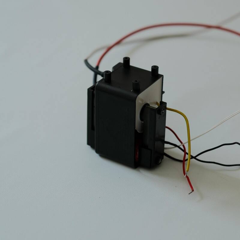
Understanding EMI Generation in Flyback Transformers
dv/dt and di/dt Transients as Primary Radiated EMI Sources
Rapid voltage transitions (dv/dt) and current spikes (di/dt) during flyback transformer switching cycles generate intense electromagnetic fields—making them the dominant sources of radiated EMI. Faster switching speeds amplify high-frequency harmonics, pushing emissions into problematic RF bands. Minimizing the physical area of high-dv/dt switching node loops and incorporating properly tuned snubber circuits are two of the most effective ways to suppress parasitic oscillations that drive these emissions.
Parasitic Coupling Paths: Interwinding Capacitance and Leakage Inductance Effects
Interwinding capacitance forms an unintentional conduction path for common-mode noise between primary and secondary windings. Meanwhile, leakage inductance stores energy during switch-off, leading to voltage overshoot and resonant ringing. Together, they create coupled resonant circuits that propagate EMI via both conducted and radiated paths. Optimizing transformer geometry—such as using interleaved windings or integrating Faraday shields—disrupts these parasitic couplings without compromising power transfer efficiency.
Flyback Transformer Design Strategies for EMI Suppression
Shielded Windings and Cancellation Techniques for Common-Mode Noise
Electrostatic shields embedded between primary and secondary windings redirect displacement currents away from sensitive circuit nodes, significantly reducing capacitive coupling—the main radiated EMI pathway. Transformer coupling simulations published in IEEE Transactions on Power Electronics (2024) show ≥10 dB reduction in common-mode (CM) noise with shielded configurations. When combined with cancellation techniques—like opposing winding phases or balanced turns ratios—these shields break resonant loops that otherwise amplify CM emissions. For instance, a counter-wound auxiliary winding can neutralize capacitive currents in the main transformer, delivering 15 dB attenuation at 30 MHz.
Optimized Winding Order and Layer Geometry to Reduce Capacitance–Leakage Trade-offs
Strategic winding arrangements help resolve the inherent tension between interwinding capacitance and leakage inductance. A sandwiched secondary design (P-S-S-P configuration) reduces primary-to-secondary capacitance by 40% compared to conventional layer stacking, per findings in the Journal of Power Electronics (2023). Progressive layer widths—narrower at high-impedance nodes—lower leakage inductance by 25% while preserving low capacitance. Replacing round wire with interleaved foil windings further shrinks field emission surfaces, cutting near-field EMI by 8–12 dB across 50–100 MHz. Fractional-turn geometries also eliminate high-dv/dt hotspots at winding edges.
Circuit-Level Filtering and Impedance Management
X/Y Capacitors, CM Chokes, and Snubbers for Radiated EMI Control
Effective radiated EMI control in flyback transformer circuits relies on coordinated impedance management and filtering. X capacitors shunt differential-mode noise between line conductors; Y capacitors divert common-mode currents from line-to-ground paths. Common-mode (CM) chokes introduce high impedance to CM currents using magnetically coupled windings—achieving 20–40 dB attenuation above 1 MHz when correctly sized. RC or RCD snubbers dampen voltage spikes caused by leakage inductance, suppressing high-frequency ringing by up to 70%. To maximize effectiveness:
- Place X/Y capacitors as close as possible to noise sources
- Locate CM chokes directly at transformer interfaces
- Tune snubber time constants to match transformer switching dynamics
This layered strategy minimizes resonant interactions and supports reliable compliance with CISPR 32 Class B radiated emissions limits.
PCB Layout Best Practices for Flyback Transformer EMI Mitigation
Minimizing High-dv/dt Loop Area and Ground Return Path Discontinuities
High dv/dt transients in flyback transformer circuits generate strong electromagnetic fields—where radiated emission intensity scales directly with loop area. To minimize this, place switching transistors adjacent to the transformer and route high-current traces with ≤5 mm separation to reduce magnetic coupling paths. Equally critical is maintaining continuous ground return paths: fragmented ground planes introduce impedance discontinuities that can elevate common-mode noise by up to 20 dB, per CISPR 32 Class B benchmark data. Use multi-via stitching every λ/10 along ground traces to suppress voltage spikes, avoid right-angle trace bends, and—for multi-layer boards—stack adjacent power and ground planes to shrink loop area by 40–60% versus single-layer alternatives.
FAQ
What is the main source of EMI in flyback transformers?
The primary sources of EMI in flyback transformers are the dv/dt and di/dt transients during switching cycles, which generate intense electromagnetic fields.
How can interwinding capacitance affect EMI generation?
Interwinding capacitance provides a conduction path for noise between windings, contributing to both conducted and radiated EMI.
What role do shields play in EMI suppression?
Shields embedded within transformer windings reduce capacitive coupling, which is a significant pathway for radiated EMI, and help break resonant loops that amplify noise.
How can PCB layout affect EMI in flyback transformers?
Effective PCB layouts minimize radiated emission by reducing high-dv/dt loop areas and maintaining continuous ground paths to prevent noise elevation.